Eurolab
-
Electrical and Electromagnetic Testing-
Magnetic Field Testing-
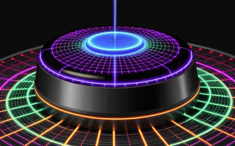
Electromagnetic Field Mapping in Electrical Devices
We provide comprehensive solutions designed to help our clients mitigate risks, enhance performance, and excel in key areas such as quality, health & safety, environmental sustainability, and social responsibility.
Discover
For many years, our organization has been operating successfully, boasting modern laboratories that meet international standards. These laboratories are equipped with the latest technology devices and equipment, and we have built a strong team of experienced and trained personnel to operate them.
DiscoverWelcome to Eurolab, your partner in pioneering solutions that encompass every facet of life. We are committed to delivering comprehensive Assurance, Testing, Inspection, and Certification services, empowering our global clientele with the ultimate confidence in their products and processes.
Discover
-
Electrical and Electromagnetic Testing-
Magnetic Field Testing-
Electromagnetic Field Mapping in Electrical DevicesElectromagnetic Field Mapping in Electrical Devices: A Comprehensive Guide
Electromagnetic fields (EMFs) are a fundamental aspect of electrical devices, playing a crucial role in their operation and performance. EMFs are created when electric currents flow through conductors, generating magnetic fields that can interact with other components within the device. Understanding and mapping these electromagnetic fields is essential for designing and optimizing electrical systems.
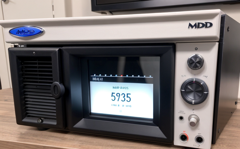
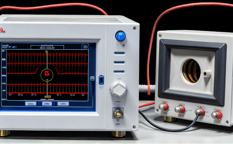
Electromagnetic field mapping involves measuring and visualizing the distribution of EMFs within a device or system. This process requires specialized tools and techniques to capture the spatial and temporal characteristics of the EMF. There are several methods for mapping EMFs, including:
MDR Testing and Compliance
MDR Testing and Compliance: A Comprehensive Guide The Medical Device Regulation (MDR) is a comprehe...
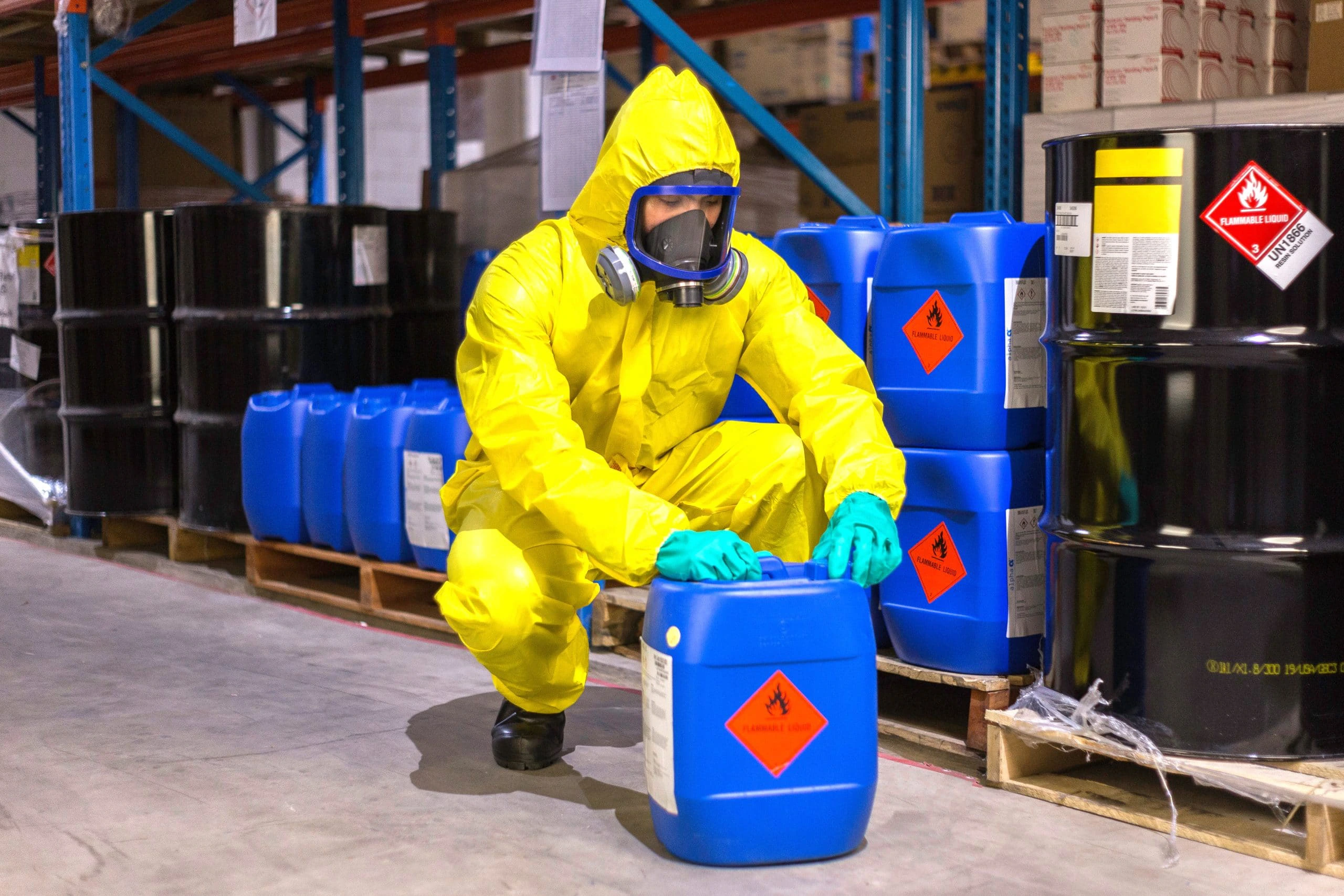
Chemical Safety and Certification
Chemical safety and certification are critical in ensuring the safe management of products and proce...
Electrical and Electromagnetic Testing
Electrical and Electromagnetic Testing: A Comprehensive Guide Introduction Electrical and electrom...
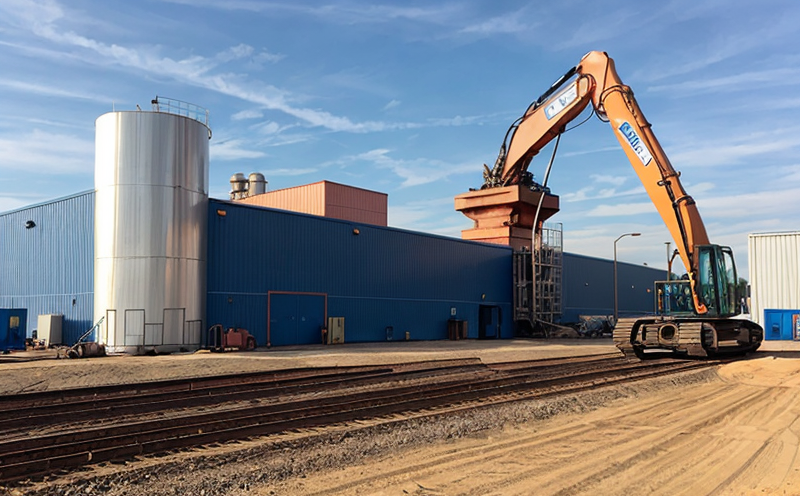
Industrial Equipment Certification
Industrial equipment certification is a critical process that ensures industrial equipment meets spe...

Environmental Simulation Testing
Environmental Simulation Testing: A Comprehensive Guide In todays world, where technology is rapidl...

Aviation and Aerospace Testing
Aviation and Aerospace Testing: Ensuring Safety and Efficiency The aviation and aerospace industr...
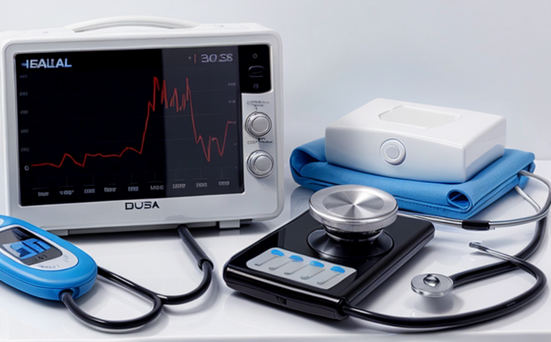
Healthcare and Medical Devices
The Evolution of Healthcare and Medical Devices: Trends, Innovations, and Challenges The healthcare...

Transportation and Logistics Certification
Transportation and Logistics Certification: A Comprehensive Guide The transportation and logistics ...

Agricultural Equipment Certification
Agricultural equipment certification is a process that ensures agricultural machinery meets specific...

Construction and Engineering Compliance
Construction and Engineering Compliance: Ensuring Safety, Quality, and Regulatory Adherence In the ...

Cosmetic Product Testing
The Complex World of Cosmetic Product Testing The cosmetics industry is a multi-billion-dollar ma...

Railway Industry Compliance
Railway Industry Compliance: Ensuring Safety and Efficiency The railway industry is a critical comp...

Fire Safety and Prevention Standards
Fire Safety and Prevention Standards: Protecting Lives and Property Fire safety and prevention stan...

Trade and Government Regulations
Trade and government regulations play a vital role in shaping the global economy. These regulations ...

Pharmaceutical Compliance
Pharmaceutical compliance refers to the adherence of pharmaceutical companies and organizations to l...

Energy and Sustainability Standards
In today’s rapidly evolving world, businesses face increasing pressure to meet global energy a...
NEBS and Telecommunication Standards
Network Equipment Building System (NEBS) and Telecommunication Standards The Network Equipment Bu...

Product and Retail Standards
Product and Retail Standards: Ensuring Quality and Safety for Consumers In todays competitive marke...

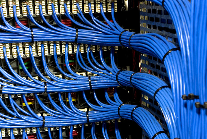
IT and Data Center Certification
IT and Data Center Certification: Understanding the Importance and Benefits The field of Informatio...

Electromechanical Safety Certification
Electromechanical Safety Certification: Ensuring Compliance and Protecting Lives In todays intercon...
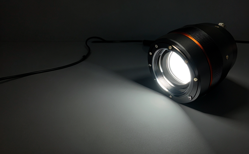
Lighting and Optical Device Testing
Lighting and Optical Device Testing: Ensuring Performance and Safety Lighting and optical devices a...

Food Safety and Testing
Food Safety and Testing: Ensuring the Quality of Our Food As consumers, we expect our food to be sa...

Consumer Product Safety
Consumer Product Safety: Protecting Consumers from Harmful Products As a consumer, you have the rig...

Environmental Impact Assessment
Environmental Impact Assessment: A Comprehensive Guide Environmental Impact Assessment (EIA) is a c...

Military Equipment Standards
Military Equipment Standards: Ensuring Effectiveness and Safety The use of military equipment is a ...

Hospitality and Tourism Certification
Hospitality and Tourism Certification: Unlocking Opportunities in the Industry The hospitality and ...

Automotive Compliance and Certification
Automotive Compliance and Certification: Ensuring Safety and Efficiency The automotive industry is ...
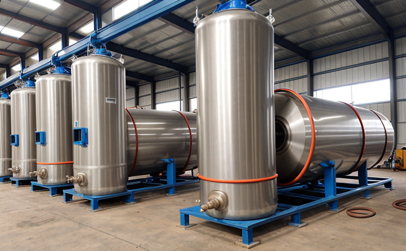
Pressure Vessels and Installations Testing
Pressure Vessels and Installations Testing Pressure vessels are a critical component of various ind...

Battery Testing and Safety
Battery Testing and Safety: A Comprehensive Guide As technology continues to advance, battery-power...
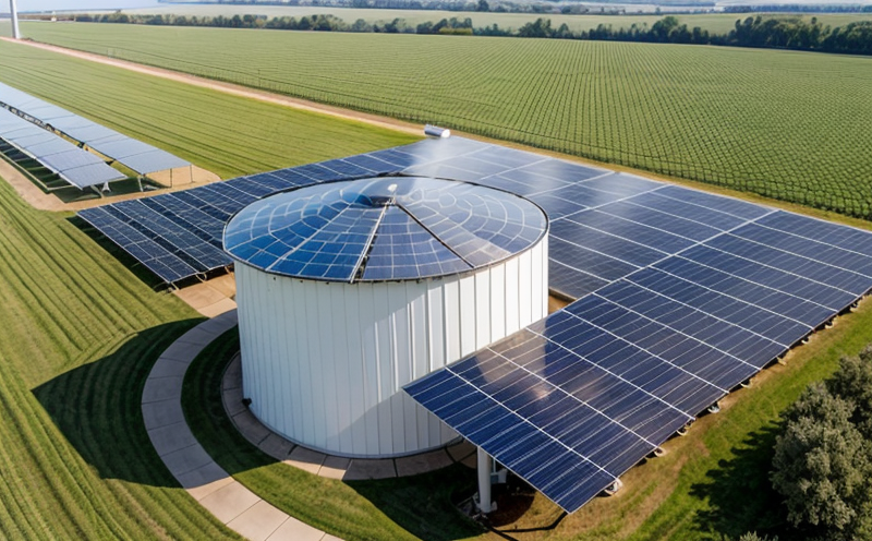
Renewable Energy Testing and Standards
Renewable Energy Testing and Standards: Ensuring a Sustainable Future The world is rapidly transiti...