Signal Integrity Testing in Multi-Layer PCB Designs: Ensuring Reliable Data Transfer
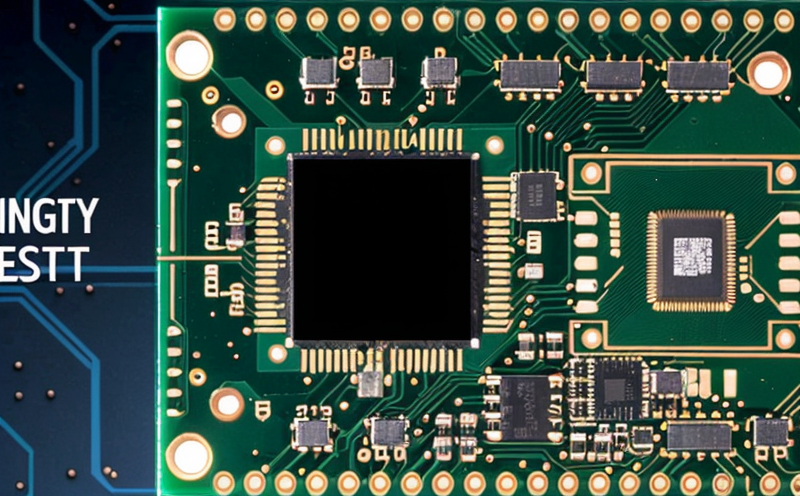
As electronic devices continue to shrink in size while increasing in complexity, multi-layer printed circuit board (PCB) designs have become the norm. These boards are essential for ensuring that high-speed signals are transmitted efficiently and accurately, but they also introduce new challenges for designers and manufacturers. One of these challenges is signal integrity testing, which involves verifying that the electrical signals on a PCB meet certain specifications and standards.
Signal integrity refers to the quality and reliability of an electrical signal as it travels through a circuit or system. In a multi-layer PCB design, signal integrity is critical because high-speed signals can be easily degraded by various factors such as electromagnetic interference (EMI), Crosstalk, Reflections, and Transmission Line Effects. If these issues are not addressed, they can lead to errors in data transfer, communication failures, and even equipment damage.
Signal Integrity Testing Methods
There are several methods for signal integrity testing, including:
Time-Domain Reflectometry (TDR): This method involves injecting a high-speed pulse into the circuit and measuring the reflections that return. TDR is used to measure impedance discontinuities, such as shorts or opens.
Frequency-Domain Analysis (FSA): This method involves analyzing the frequency response of a signal to determine its integrity. FSA can identify resonance frequencies and other issues that may affect signal quality.
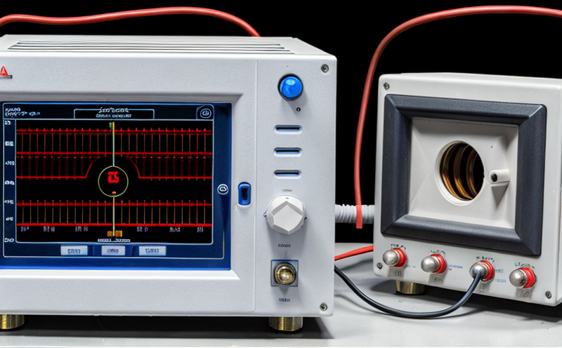
Eye Diagram Analysis: The eye diagram analysis provides a graphical representation of the eye pattern, which is a measure of signal quality. It is used to evaluate jitter, duty cycle distortion, and other effects on signal quality.
Key Parameters in Signal Integrity Testing
Several key parameters are crucial in signal integrity testing:
Rise Time: This refers to the time it takes for a signal to rise from 10 to 90 of its maximum amplitude.
Fall Time: This refers to the time it takes for a signal to fall from 90 to 10 of its maximum amplitude.
Jitter: This is a measure of the random variation in the timing of a signal. High jitter can lead to errors in data transfer.
Crosstalk: This occurs when a signal on one wire affects another nearby wire.
Signal Integrity Testing in Multi-Layer PCB Designs
When it comes to multi-layer PCB designs, signal integrity testing becomes even more critical due to the increased complexity and density of the board. Here are some key considerations:
Crosstalk and Coupling: In multi-layer PCB designs, crosstalk and coupling can occur between adjacent wires or between wires and ground planes. This can lead to signal degradation and errors in data transfer.
Crosstalk occurs when a signal on one wire affects another nearby wire due to electromagnetic coupling. It is measured as the ratio of the voltage induced on the affected wire to the original signal.
Coupling refers to the energy transferred between two or more adjacent wires.
Transmission Line Effects: In high-speed circuits, transmission line effects can become significant. These include:
Reflections: When a signal encounters a discontinuity in the transmission line (e.g., a change in impedance), it reflects back into the source.
Delay: Signals travel at different speeds through different types of transmission lines (e.g., copper vs. FR4).
Dispersion: The spreading out of a signal as it travels through a transmission line.
Signal Integrity Testing Tools and Techniques
Several tools and techniques are available for signal integrity testing, including:
Vector Network Analyzers (VNAs): VNAs measure the reflection coefficient (S11) and insertion loss (S21) of a circuit.
Signal Integrity Simulation Software: Commercial software such as ADS, Simbeano, and Sigxfer can model complex circuits and simulate signal integrity issues.
QA Section
Q: What is signal integrity, and why is it critical in multi-layer PCB designs?
A:
Signal integrity refers to the quality and reliability of an electrical signal as it travels through a circuit or system. In multi-layer PCB designs, signal integrity is critical because high-speed signals can be easily degraded by various factors such as EMI, Crosstalk, Reflections, and Transmission Line Effects.
Q: What are some common signal integrity testing methods?
A: Time-Domain Reflectometry (TDR), Frequency-Domain Analysis (FSA), and Eye Diagram Analysis are three common signal integrity testing methods.
Q: How does crosstalk affect signal integrity in multi-layer PCB designs?
A:
Crosstalk can lead to signal degradation and errors in data transfer. It occurs when a signal on one wire affects another nearby wire due to electromagnetic coupling.
Q: What is transmission line effect, and how does it impact signal integrity?
A: Transmission line effects refer to the changes that occur as a signal travels through a transmission line (e.g., reflections, delay, and dispersion).
Q: Are there any tools or techniques available for signal integrity testing?
A:
Yes, several tools and techniques are available for signal integrity testing, including vector network analyzers (VNAs), signal integrity simulation software, and measurement equipment.
Q: How can I ensure that my multi-layer PCB design meets signal integrity standards?
A: To ensure that your multi-layer PCB design meets signal integrity standards, you should perform thorough signal integrity analysis using commercial software or manual calculations. Additionally, consider performing TDR, FSA, and eye diagram analysis to identify potential issues.
Q: Can I use manual calculations for signal integrity analysis, or is commercial software required?
A:
While manual calculations can be used for simple cases, commercial software such as ADS, Simbeano, and Sigxfer are recommended for complex circuits. These tools can model the behavior of high-speed signals and simulate various scenarios to ensure reliable data transfer.
Q: What is the relationship between rise time and signal integrity?
A: Rise time refers to the time it takes for a signal to rise from 10 to 90 of its maximum amplitude. Faster rise times can lead to increased jitter, which can impact signal quality and reliability.
Q: Can I use eye diagram analysis alone to evaluate signal integrity in my multi-layer PCB design?
A:
While eye diagram analysis is an excellent tool for evaluating signal integrity, it should be used in conjunction with other methods such as TDR and FSA. Each method provides unique information about the circuits behavior, which can help identify potential issues.
Q: How often should I perform signal integrity testing on my multi-layer PCB design?
A: Signal integrity testing should be performed throughout the design process, from initial prototyping to final production. This will help ensure that your design meets signal integrity standards and is reliable for high-speed applications.
Signal Integrity Testing in Multi-Layer PCB Designs: Conclusion
Signal integrity testing is an essential aspect of multi-layer PCB design, particularly for high-speed circuits. By understanding key parameters such as crosstalk, transmission line effects, and rise time, designers can take steps to minimize signal degradation and ensure reliable data transfer. Commercial software, measurement equipment, and simulation techniques are available to aid in signal integrity analysis and testing. By combining these tools with a thorough understanding of signal integrity principles, designers can create high-speed circuits that meet the demands of modern electronics applications.